New 3D design for mobile microbatteries
In the race towards miniaturization, a French-US team—mostly involving researchers from the CNRS, Université de Lille, Université de Nantes and Argonne National Laboratory (US) as part of the Research Network on Electrochemical Energy Storage (RS2E)1 —has succeeded in improving the energy density of a rechargeable battery without increasing its size (limited to a few square millimeters in mobile sensors). This feat was achieved by developing a 3D structure made of microtubes, the first step towards producing a complete microbattery. The first experiments have demonstrated the excellent conductivity of the battery's solid electrolyte, whose highly encouraging performance is published in the journal Advanced Energy Materials on October 11, 2016.
- 1Launched in 2011 at the initiative of the CNRS and the Ministry of National Education, Higher Education and Research, this network is co-directed by Jean-Marie Tarascon, today professor at the Collège de France, and Patrice Simon, professor at the Université de Toulouse III - Paul Sabatier.
In the era of connected devices, intelligent connected microsensors require miniature embedded energy sources with great energy density. For ultra-thin—or planar—microbatteries, increased energy density means using thicker layers of materials, which has obvious limitations. A second method—used by the authors of the publication—consists in machining a silicon wafer2
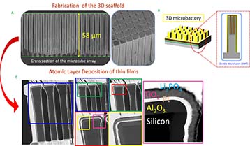
and producing an original 3D structure made of simple or double microtubes. 3D batteries keep their 1mm2 footprint area, but develop a specific area of 50 mm2—an enhancement factor of 50! These robust microtubes are large enough (of the order of the micron) to be coated with multiple layers of functional materials3
.
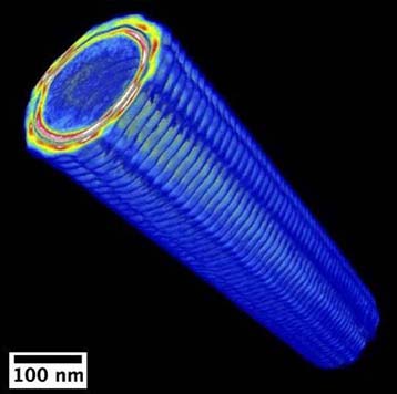
The main technological challenge consisted precisely in depositing the different materials that make up the rechargeable battery in thin and regular layers on these complex 3D structures. Using the cutting edge technology of Atomic Layer Deposition (ALD), the materials perfectly took on the 3D shape of the template without blocking the tube structures. In this way the researchers created an insulating thin film, a current collector, a negative electrode, and a solid electrolyte. The various analyses and characterizations (synchrotron X-ray nanotomography and transmission electron microscopy4
) show that the successive layers are of excellent quality, showing conformality of nearly 100%. The interfaces are clean (no interdiffusion between the different chemical elements), with no pinholes, cracks, or fissures detected.
Lithium phosphate, the electrolyte of this future 3D microbattery, is in solid form5
. After depositing it using the same ALD technology, researchers showed that it has a high electrochemical stability window (4.2 V), high ionic conductivity, and low thickness (10 to 50 nm), which generates low surface resistance, all of which are very encouraging for the future performance of the 3D battery.
The next step will consist in using ALD to develop thin films of positive electrode materials in order to create the first functional 3D prototypes, which will certainly offer much greater performance than today's planar microbatteries.
This research has involved researchers from the Institut d'électronique, de microélectronique et de nanotechnologie (CNRS/Université de Lille/Isen Lille/Université Valenciennes Hainaut-Cambresis/Ecole centrale de Lille), the Unité de catalyse et de chimie du solide (CNRS/Université de Lille/ ENSV Lille/Ecole centrale de Lille/Université Artois), the Institut des matériaux de Nantes Jean Rouxel (CNRS/Université de Nantes), the Laboratoire réactivité et chimie des solides (CNRS/Université Picardie Jules Verne), and the Argonne National Laboratory in the US.
This work is patented: "Substrat microstructuré," C. Lethien, P. Tilmant, E. Eustache, N. Rolland, T. Brousse, WO2015/052412 A1. The study was funded by the ANR, the DGA, the Renatech network, and the RS2E network.


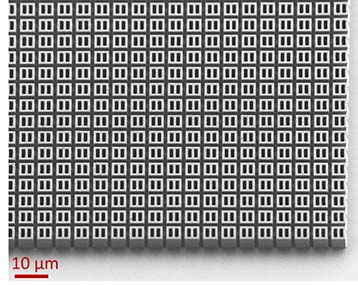
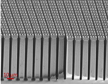
Images of double microtubes obtained by scanning electron microscopy.

Images of double microtubes obtained by scanning electron microscopy.

Synchrotron X-Ray Tomographic analysis of one microstructure covered with multiple layers of materials.
- 2A wafer is a thin disc of semiconducting material, such as silicon, the material of choice in the microelectronics industry.
- 3The successive layers of materials are the very essence of a battery.
- 4X-ray nanotomography is a non-destructive technique that reconstructs cross-section images of three-dimensional objects on the nanometric scale. Transmission electron microscopy is a microscopy technique in which a beam of electrons is "transmitted" through a very thin sample.
- 5A solid electrolyte escapes the limitations of liquid electrolytes: flammability, evaporation of solvents, potential leaks.
Atomic layer deposition of functional layers for on Chip 3D Li-ion all solid state microbattery. M. Létiche, E. Eustache, J. Freixas, A. Demortière, V. De Andrade, L. Morgenroth, P. Tilmant, F. Vaurette, D. Troadec, P. Roussel, T. Brousse, C. Lethien. Advanced Energy Materials, October 11, 2016. View web site


